Analog Design Intern at Melexis
Melexis, Ypres · Jul–Aug 2025
The current sensor product relies on an analog output amplifier to provide a conditioned signal proportional to the measured current. The existing design had a bandwidth limitation that restricted the sensor's ability to accurately capture high-frequency current transients. The objective of this internship was to design a new output amplifier achieving a substantially higher bandwidth, while meeting a demanding set of specifications for gain accuracy, noise, offset, slew rate, output impedance, and stability across a wide range of process, voltage, temperature corners, and capacitive loads.
Due to the schematic complexity required and the fact that the target bandwidth was pushing the limits of the technology node, the scope focused on transistor-level schematic development and a complete simulation suite. Layout considerations such as EMC immunity were descoped, though block size and matching were reasoned about throughout.
Circuit
The amplifier is a three-stage design using cascode (Ahuja) compensation. It consists of a folded cascode core amplifier, a high-current drive stage, and an RC feedback network. The top-level ‘outbuffer’ block below contains the fixed RC feedback network and an identical copy connected to the reference voltage. A split cascode capacitor connects the output to the differential signal between the CoreAmp and OutDrive stages.
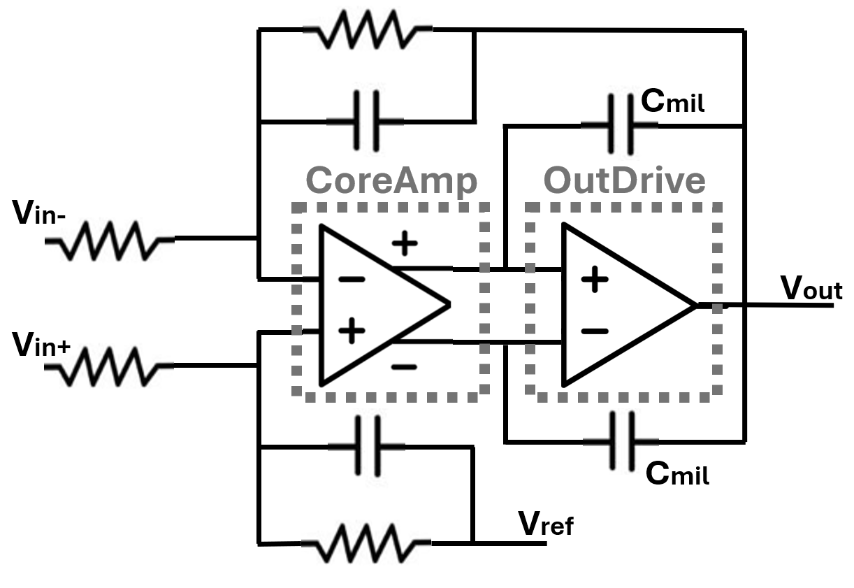
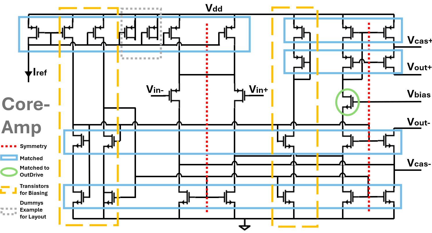
The CoreAmp is a folded cascode with a pMOS input pair. The differential output is split into Vout+ and Vout-, feeding the drive stage. Layout annotations indicate transistors that should be matched in a common-centroid arrangement (blue) and symmetry axes to carry through to layout (red dashed).
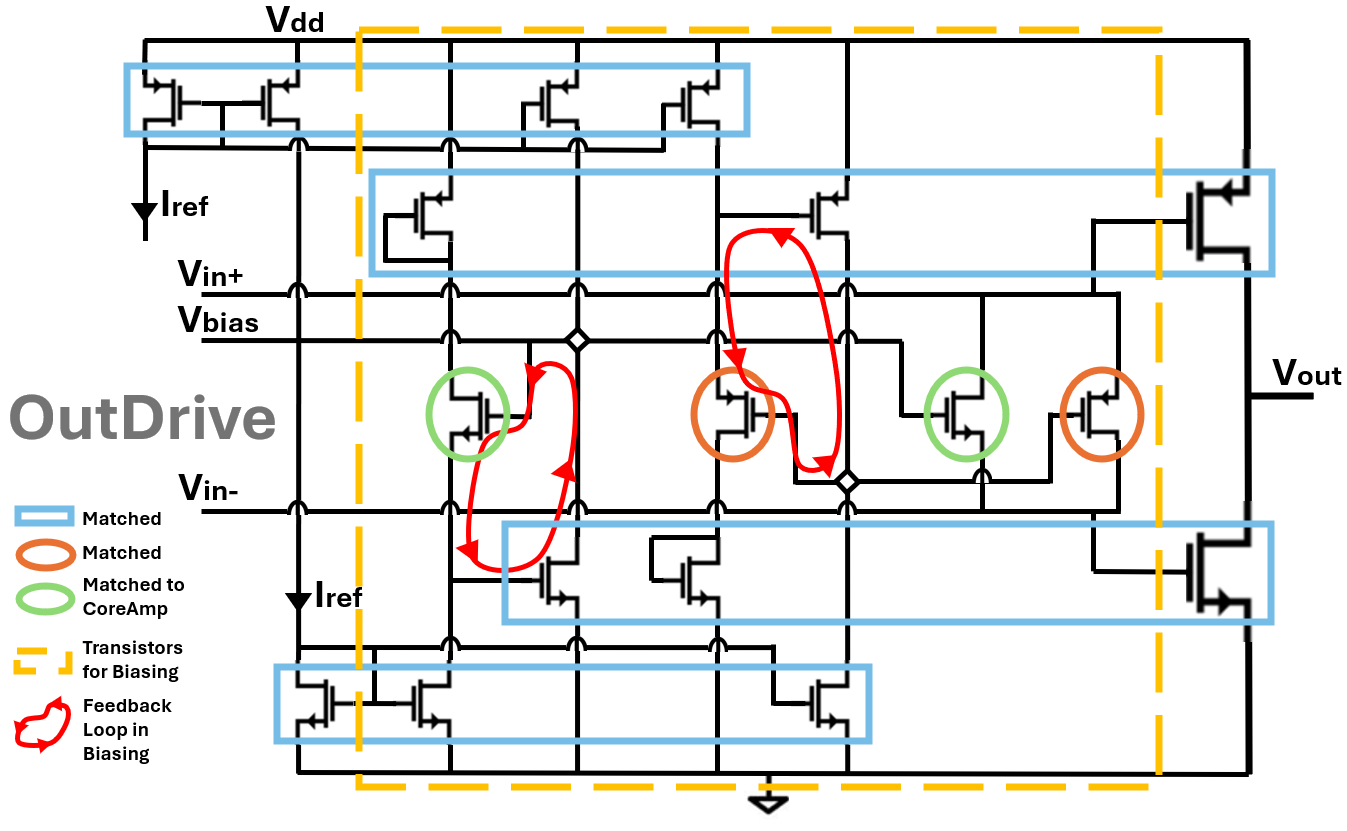
The OutDrive stage uses self-biased large pMOS and nMOS transistors to deliver the current needed for the highest capacitive loads. Rather than biasing both from a fixed voltage, the design copies a known reference current through matched transistors and uses an internal feedback loop to transfer the resulting gate voltage to the large devices. This keeps the biasing network current-efficient while allowing the drive strength to be set via a single multiplier ratio.
Compensation and Temperature Biasing
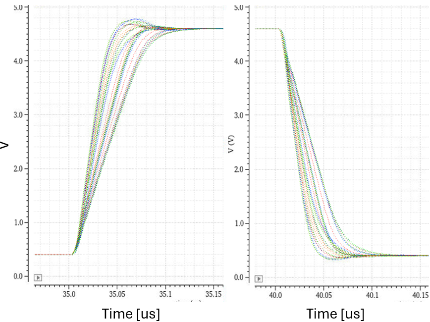
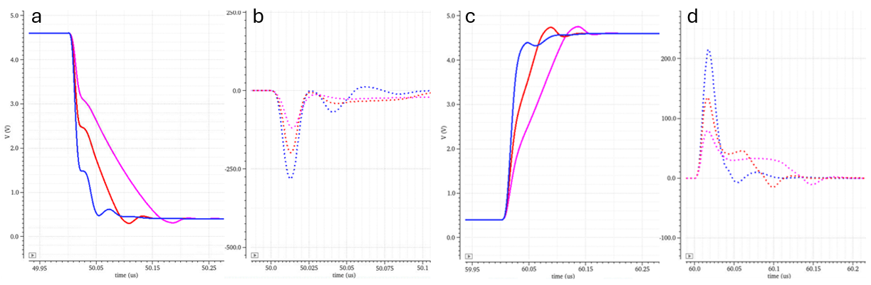
The initial design used Miller compensation. Transient simulations revealed that this caused oscillation-like behavior in the step response, visible as a steep initial slope from the direct feedforward path through the Miller cap followed by a slower settling. Switching to cascode (Ahuja) compensation resolved this. The compensation capacitor was then split into two equal capacitors connecting to Vcas+ and Vcas- to further improve the step and sine response. Because several types of capacitors were connected in parallel, the effective capacitance remains approximately constant over the voltage bias range while maintaining area efficiency.
High-temperature corners consistently failed for reasonable bias currents while low-temperature corners showed margins. A temperature-dependent bias current, combined with a static reference already available on the chip, was used to track the required current over temperature. This solved the high-temperature corners without wasting current at nominal conditions, and its negative temperature coefficient also benefited a neighboring block on the chip, keeping total chip current more constant over temperature.
Simulations
The full simulation suite covered all specifications across process corners, supply voltage, temperature (−40°C to 175°C), common-mode input voltage, and capacitive loads from 0 pF to 242 pF, totaling over a thousand corner-and-operating-condition combinations. The following tests were run:
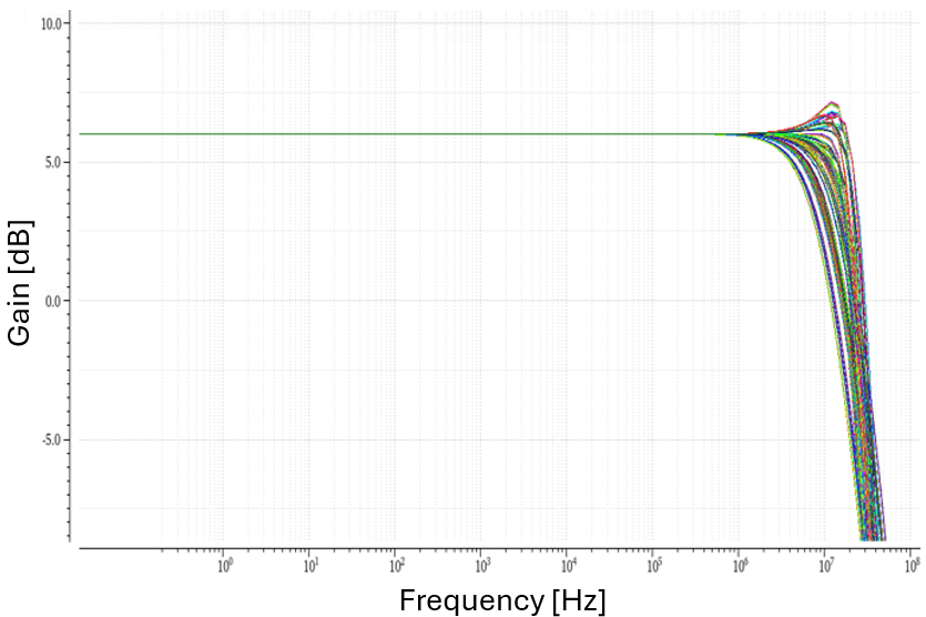
- —AC, DC, stability, and noise: combined test covering small-signal gain across frequency, phase margin, gain margin, and integrated noise, run over all corners and operating conditions.
- —Output impedance: transient simulation varying Rload for minimum, typical, and maximum common-mode input voltage.
- —Linearity: DC sweep of the differential input across the full input range to compute the maximum linearity error as a percentage of full scale.
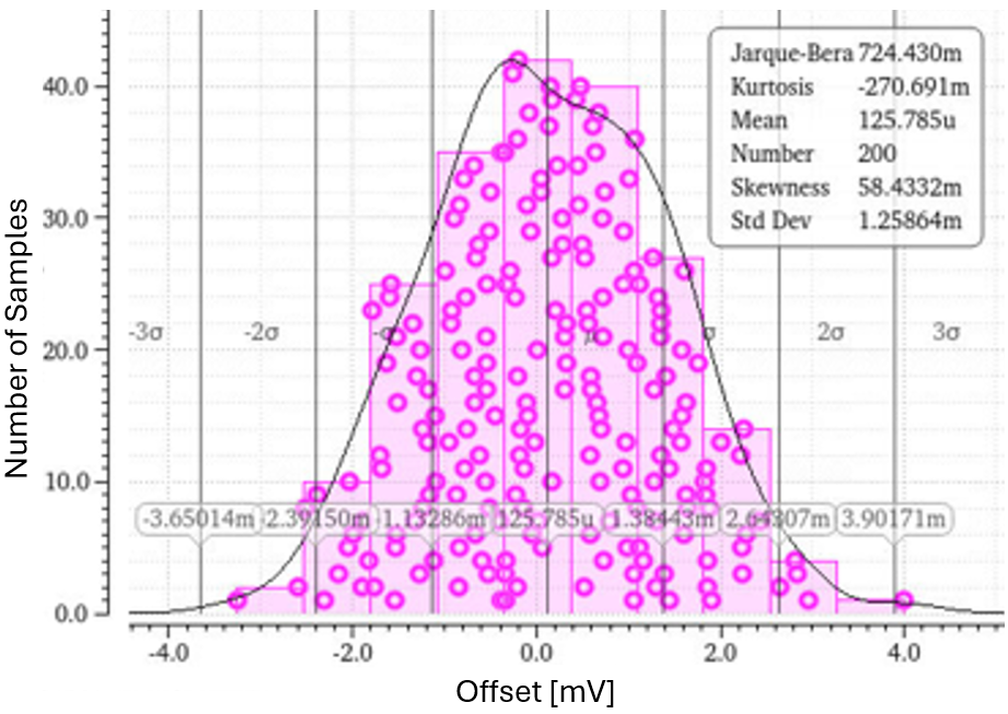
- —DC offset and temperature drift: Monte Carlo simulation (200 samples) measuring the output voltage at zero differential input. Temperature drift evaluated by sweeping 25°C, −40°C, 90°C, and 175°C across the Monte Carlo samples and taking the largest deviation. Offset quantified as mean ± 6σ.
- —Transient behavior: combined transient test for start-up time, step response, slew rate, propagation delay (10% output), and settling time (90% output), as well as sine-wave response, all in a single simulation run.