Dynamic Biasing for Analog Circuit Stability in a LEO Radiation and Thermal Environment
Harsh Environment Electronics Capstone Project with Gabriel Tetrault · Columbia University · 2025
Low Earth orbit is the most common satellite orbit, and it is harsh on electronics: total ionizing dose (TID) radiation gradually shifts MOSFET threshold voltages, while wide thermal cycling over each orbit moves every bias-dependent parameter along with it. This is a particular problem for low-cost missions built from commercial off-the-shelf (COTS) parts, where custom rad-hard silicon is not an option. The objective of this project was to design circuits from generic components and let the architecture itself correct for threshold voltage degradation and transconductance fluctuations under radiation and temperature swings.
Approach
The chosen perspective on dynamic biasing is the intentional alteration of one or more biasing parameters in response to circuit parameters that have unintentionally changed, as maintenance of a constant output. In other words: a feedback loop that senses the drift and rebiases the circuit continuously, rather than duty-cycling power to slow the damage.
The stress envelope was made concrete with SPENVIS data for a five-year LEO mission, giving the total ionizing dose behind a minimal aluminium shielding thickness, and the Krantz equation was used to translate that dose into an expected threshold voltage shift. Two feedback-based circuits were then designed around this envelope: one that creates a stable bias current, and one that keeps the transconductance of an OTA input pair constant.
The Two Circuits
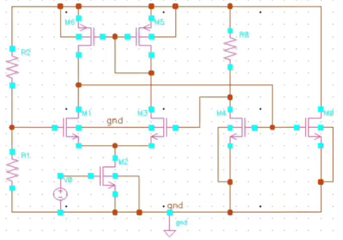
The bias current circuit extends a simple resistor-biased current source with a differential pair that compares the actual operating point against a reference and feeds the difference back to the output branch, so the delivered current stays fixed as the threshold voltage walks away.
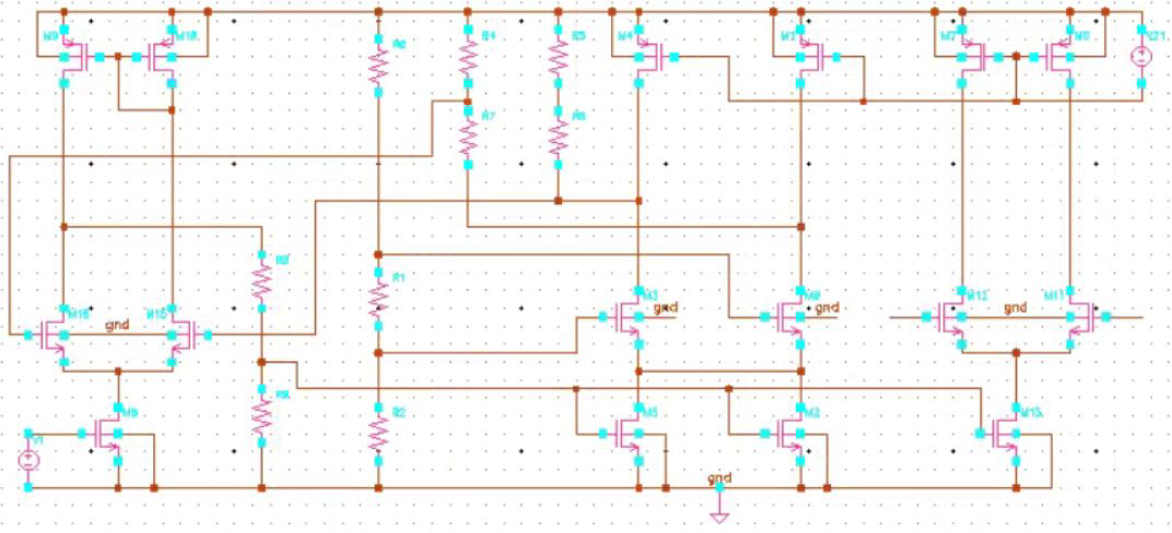
The constant-gm circuit uses the fact that gm is the derivative of drain current with respect to gate voltage: a small fixed voltage difference is applied across two matched replica branches, the resulting current difference is measured as a direct probe of the input pair's gm, and the feedback loop adjusts the tail bias until that measured gm equals the desired value.
Results
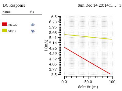
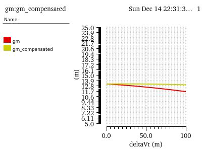
Both circuits were verified in Cadence Virtuoso with Spectre, applying a threshold voltage shift of 0 to 100 mV as a gate-voltage offset and sweeping temperature from −20 °C to +50 °C, against baselines with fixed biasing. Where the uncompensated current and gm fall away steadily with the threshold shift, the compensated versions stay nearly flat across the full shift range at every simulated temperature.
Limitations
- Compensating for the threshold shift does not undo the underlying degradation: with enough accumulated dose the devices can end up permanently off, so wide-bandgap COTS parts or redundancy remain necessary for very long missions.
- The approach assumes even conditions across the die. Single-event upsets or non-uniform temperature can turn the feedback positive, which argues for a small compensation area and heat spreaders.